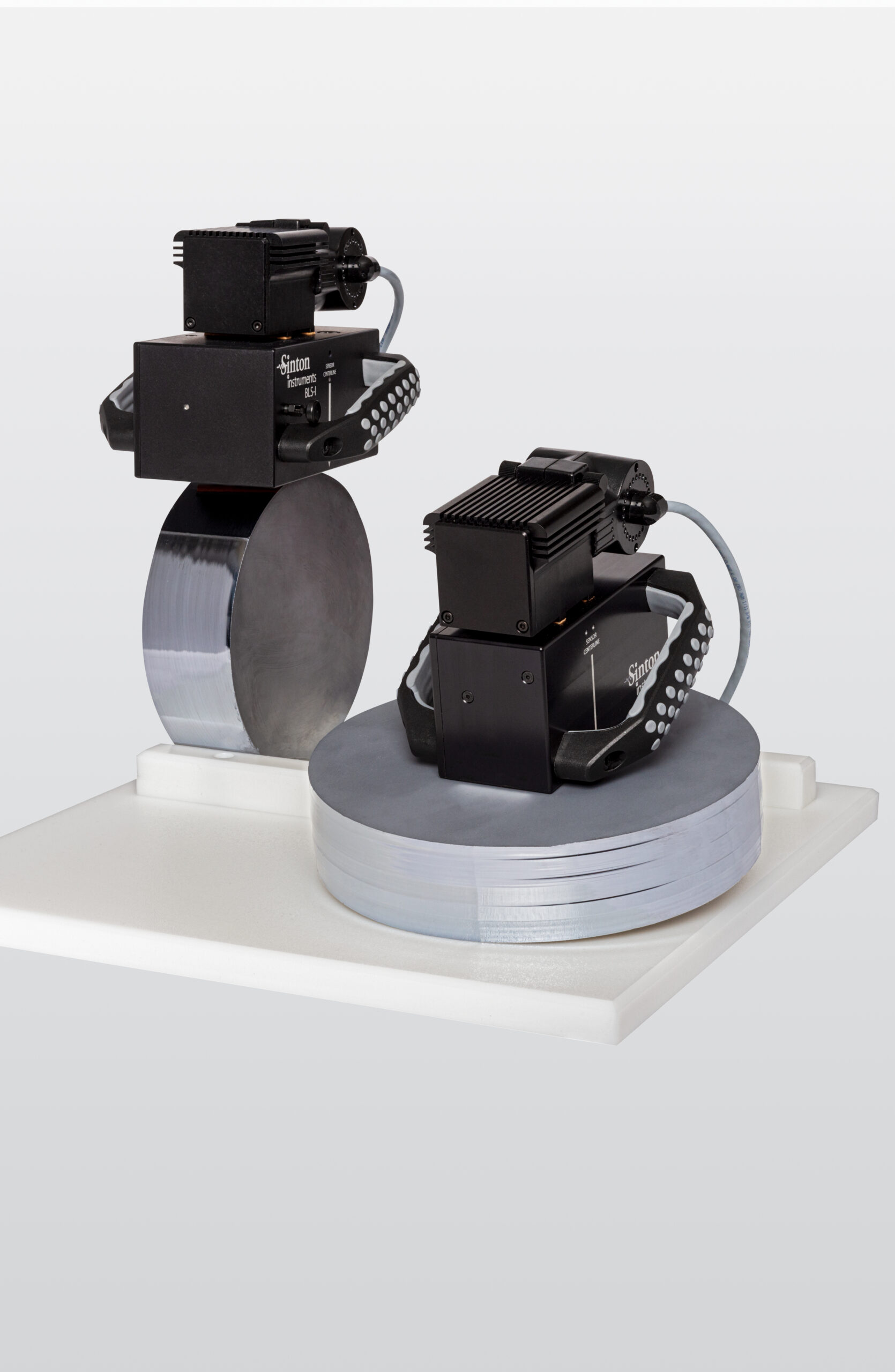
Simple and accurate contactless measurement of true bulk lifetimes on as-grown or shaped silicon. Complies with SEMI Standard PV-13.
Shock absorbing, retracting pads that conform to ingot curvature enable the BLS-I to measure any surface of as-grown or shaped ingots.
Product Overview
The BLS-I and BCT-400 measurement systems perform bulk lifetime measurements on monocrystalline or multicrystalline silicon (ingots or bricks) without requiring surface passivation. Since lifetime measurements are among the most sensitive techniques for characterizing growth and contamination defects, these tools allow you to assess silicon quality directly after growth.
For the flexibility to measure all surface types (from 150-mm diameter to flat) choose the BLS-I. For a compact tool designed to measure only flat surfaces, choose the BCT-400. The BCT-400 can also be mechanically integrated into an automation station and the software can be setup for seamless automated measurements.
System Capabilities
- Qualifying high-purity silicon with lifetimes in the 1–10+ millisecond range
- Qualifying B-Cz silicon as-grown, without special surface preparation
- Characterizing lifetime and trap density in multicrystalline blocks
- Detecting B-O defects, Fe contamination, and surface damage
- Monitoring initial material quality in Cz, FZ, multicrystalline, or UMG silicon
Further Information
For key features, specifications, and additional information, download the BLS/BCT product note (PDF – 803k).
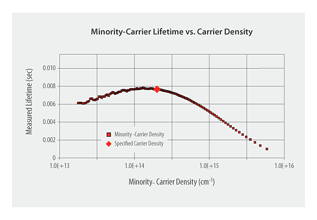
Example 1. A transient measurement of an n-type ingot with a lifetime of 8 ms.
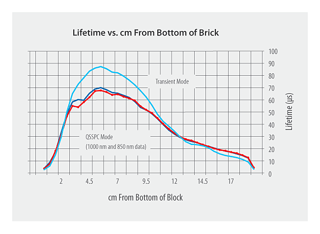
Example 2. P-type multicrystalline silicon showing the characteristic variation of lifetime from the bottom to the top of the brick. Trapping and resistivity profiles are also compiled for each measurement (not shown here)


